
Chipenomics
What the Nvidia Bear Case Gets Wrong (And Right)


The Nvidia bear case rests heavily on circular financing and useful-life discrepancies: when a chipmaker invests equity into its own customers, who then spend that money buying the chipmaker's product, the resulting revenue is not as clean as it looks on an earnings call. The critique has merit as an accounting matter, but it does not currently translate into a market-share problem. Nvidia has no direct competitor that handles both training and inference at its scale, its margin, or its ecosystem depth, and CUDA lock-in combined with years of installed base means the circular financing critique remains a balance-sheet argument rather than a competitive one. The more consequential threat to Nvidia is structural, and it originates from the demand side of its own business rather than from short sellers.
That structural pressure comes from what can be called the Nvidia tax. Every frontier lab renting compute at Nvidia's roughly 75% data-center gross margin is effectively subsidizing Nvidia's balance sheet with every token generated, and several labs have already acted on it. OpenAI is furthest along, having co-designed a chip with Broadcom, fabbed at TSMC, that ran under the internal codename Titan before its public unveiling on June 24 as Jalapeño: inference-only, tuned specifically to the large language models OpenAI already runs, and not for sale. The build-out behind it is a 10-gigawatt commitment running from the second half of 2026 through 2029, with analysts pricing the full deployment at somewhere near $350 billion, and OpenAI has said the design went from concept to tape-out in nine months. Anthropic has taken a more hedged version of the same position, pulling in Samsung, SK Hynix, and Micron as strategic partners on a custom inference chip while keeping Trainium and TPU capacity central to its plans. Broadcom is reportedly running similar co-design work with Google and Meta at the same time, which is less a signal that any one lab has cracked the problem than evidence that avoiding Nvidia's margin has become a standing item on every frontier lab's infrastructure agenda.
Vertical integration and circular financing are two sides of the same balance sheet. One is frontier labs trying to stop paying Nvidia's margin. The other is Nvidia trying to make sure the money it doesn't collect on the chip comes back through an equity stake instead.
Two companies outside the hyperscaler tier illustrate this shift with different architectural approaches. Etched, whose founders detailed their thesis on Invest Like the Best, built its Sohu chip around a specific bet: that fewer than 100 models would ultimately matter, and that those models would be similar enough mathematically to justify hand-writing kernels for transformer attention rather than building a general compiler. Sohu hard-codes attention directly into silicon as fixed-function logic, and Etched's own published figures claim roughly 62,500 tokens per second per chip on Llama 70B at batch size one, against a single H100 running vLLM at closer to 700 tokens per second under the same condition, according to Spheron's comparison of the two chips. That gap narrows considerably at production batch sizes: Spheron puts H100 throughput at roughly 5,000 tokens per second at batch 32 and 45,000 at batch 256, figures for which Etched has not published a Sohu equivalent. The same analysis is specific about what Sohu cannot run at all, including mixture-of-experts models with dynamic routing such as DeepSeek V4 and Qwen3-235B-A22B, along with multimodal, diffusion, and state-space architectures, since none of these map onto circuits built exclusively for dense transformer attention.
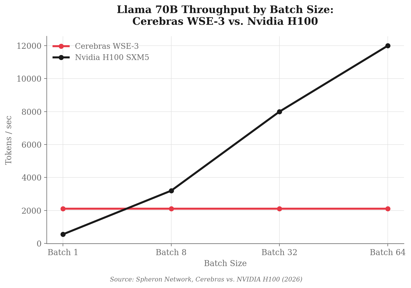
Cerebras took a different approach to the same underlying problem. Andrew Feldman's framing on The MAD Podcast describes a token's lifecycle in three stages, training, prefill, and decode, with decode bottlenecked by memory bandwidth rather than raw arithmetic, since generating each token requires moving the model's full weight set from memory to compute. Cerebras addresses this by keeping the entire model on a single wafer-scale chip with on-die SRAM rather than off-chip HBM, and per Spheron's separate comparison against Nvidia, the WSE-3 holds a fixed throughput of roughly 2,100 tokens per second on Llama 70B regardless of batch size, well above a single H100's 550 tokens per second at batch one. The H100 overtakes it by batch eight, though, and reaches roughly 12,000 tokens per second at batch 64, since GPU memory bandwidth serves batched requests in parallel in a way the WSE-3's fixed pipeline cannot. Spheron's cost modeling puts Cerebras at a flat $0.60 per million output tokens against an H100 rate that falls from $1.47 per million at batch one to roughly $0.10 per million at batch 32, placing the break-even point between two and eight concurrent requests: below that, Cerebras is cheaper, and above it, H100 is substantially cheaper. Both companies are betting that Nvidia's programmability, the feature that lets a single H100 serve almost any workload, is exactly the overhead that becomes unnecessary once a workload is narrow and stable enough to specialize against, but both comparisons also show that specialization carries a real cost in model coverage and batch flexibility.
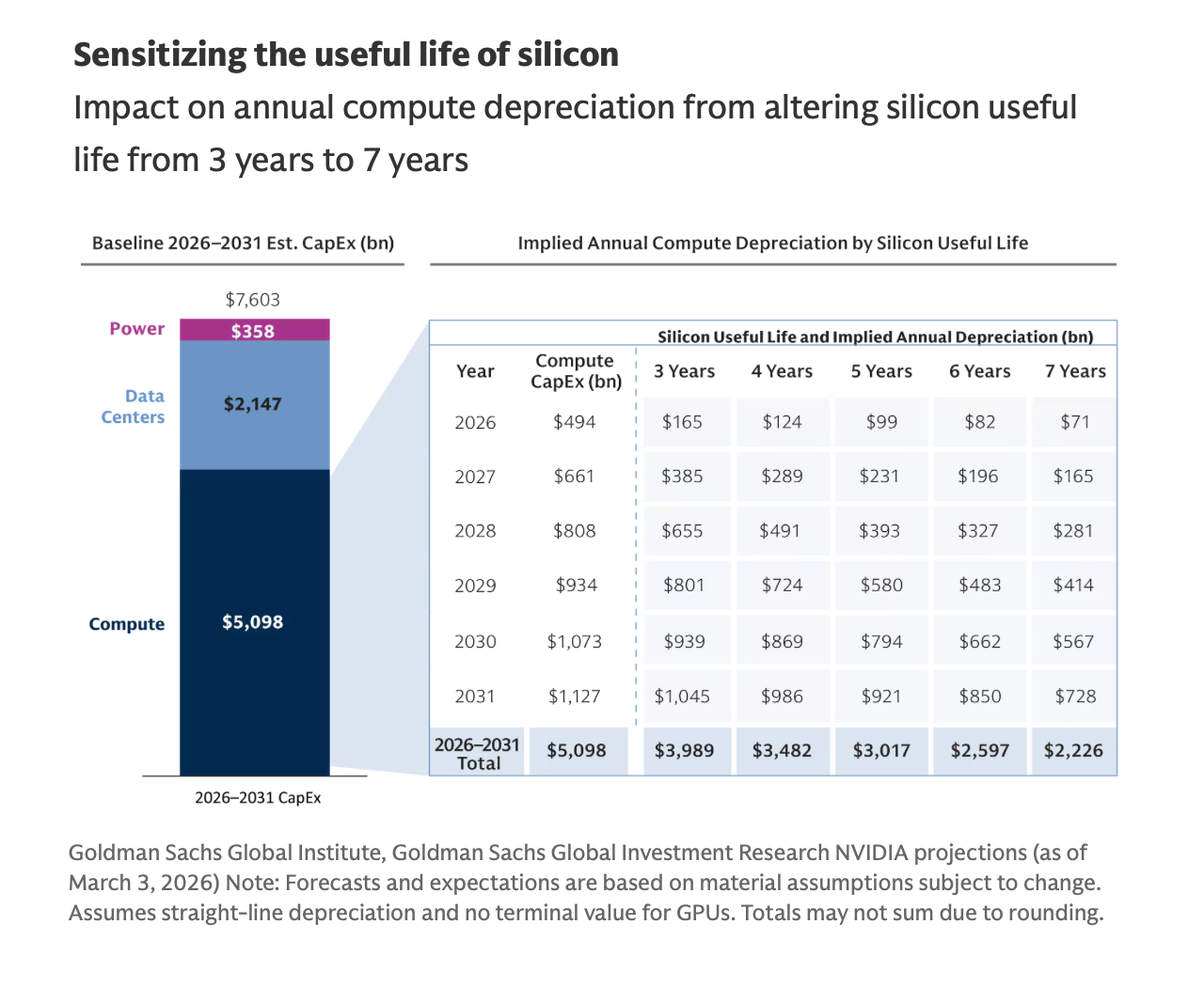
Goldman Sachs' research provides a framework for evaluating whether either approach meaningfully threatens Nvidia's position, and the relevant lens is amortization. Goldman identifies the useful life of AI silicon as the single most influential variable in aggregate AI capital expenditure, more consequential than data center costs or chip architecture mix, because the tension between rapid generational improvement and continued operational value determines how many replacement cycles the industry must fund. A chip depreciated over five years carries a fixed annual expense, and shrinking or extending that window shifts industry-wide spending by hundreds of billions of dollars. Sohu's low-voltage design is relevant here specifically because reduced thermal throttling, if it extends physical chip lifespan as the underlying physics suggests it should, would improve only one half of Goldman's useful-life equation. It would not address the second half: economic obsolescence driven by the next architectural leap. Given that Sohu already cannot serve a meaningful share of current production workloads, that obsolescence risk is more acute for a fixed-function chip than for Cerebras, whose wafer-scale design remains fully programmable and can in principle adapt to whatever architecture follows transformers, in the way an H100 can.
The amortization framework applies consistently across all three comparisons. Nvidia's advantage has never rested primarily on raw throughput. It rests on flexibility across model architecture, batch size, and workload type, and that flexibility is what determines whether a chip remains useful once the next generation of models arrives.
